 Search


- AMTE is committed to the global semiconductor and pan semiconductor high-end micro nano high-tech equipment manufacturing industry

Today, as semiconductor manufacturing continues to develop towards smaller processes and larger wafer sizes, 12 inch wafers have become the mainstream of high-end chip manufacturing. Plasma enhanced chemical vapor deposition (PECVD) is a key step in thin film deposition technology, and its process quality and equipment stability directly affect the performance and yield of the device.
12 inch PECVD is one of the key engines driving the continuation of Moore's Law, and its importance is reflected in:
1. Empowerors for improving transistor performance
In advanced process structures, depositing precise stress films to directly regulate the stress state of transistor channels is one of the core technologies for improving driving current and reducing power consumption.
2. Support points for advanced interconnect technology
With the improvement of chip integration, the number of interconnect layers can reach more than ten. The low-k/Ultra low-k dielectric film deposited by 12 inch PECVD is the key to reducing inter line capacitance, preventing signal crosstalk and delay, improving chip computing speed, and reducing power consumption. In addition, its excellent gap filling capability ensures reliable insulation of complex interconnect structures.
3. The core of improving efficiency and reducing costs
The number of chips that can be produced from a single 12 inch wafer is more than 2.5 times that of an 8-inch wafer, significantly reducing the manufacturing cost of a single chip. Meanwhile, its higher level of automation and production efficiency make it possible to produce advanced chips on a large scale and economically.
Based on the key role of 12 inch PECVD technology, Yiwen Technology closely follows the trend of industrial upgrading and officially launches the independently developed 12 inch capacitance coupled plasma enhanced chemical vapor deposition equipment (SPV 12D), providing high-performance and high stability domestic thin film deposition solutions for advanced semiconductor manufacturing. This equipment has been extensively deployed in the field of 12 inch advanced processes and is an important force in promoting the localization of 12 inch PECVD models.
First: AMTE12 inch PECVD product overview
Product Introduction
SeriC Plasma SPV 12D is a high-performance 12 inch plasma enhanced chemical vapor deposition (PECVD) thin film equipment independently developed and designed by AMTE. It aims to solve core problems such as uniformity, density, and process stability of thin film deposition in advanced processes for semiconductor integrated circuit manufacturing enterprises, and help customers achieve high-performance and high reliability integrated circuit production.
Extraordinary film uniformity: Equipped with a self-developed high-precision plasma source and reaction chamber intelligent airflow control system, it can achieve film thickness uniformity and stress matching of less than 1.5% on the entire 12 inch wafer. This means higher yield and more consistent device performance.
Wide range of material systems: Comprehensive support for the deposition of multiple critical media thin films, including:
SiO ₂ (silicon oxide): serves as a standard isolation layer and protective layer.
SiN (silicon nitride): Excellent etching stop layer and passivation layer.
SiON (silicon nitride oxide): used for anti reflective coatings and gate dielectrics.
Low k dielectric materials: help reduce RC delay and improve chip speed.
Ultra high throughput: Optimized multi chamber cluster architecture and high-speed robotic arm transmission system minimize single wafer processing cycles, significantly increase production capacity, and reduce single-chip manufacturing costs.
Excellent Particle Control and Uptime: UsingAMTE's patented chamber cleaning technology and particle control solution, wafer particle contamination is controlled at an extremely low level of<10 particles (@>0.06 μ m). Modular design and advanced fault prediction and diagnosis system ensure that the equipment has a continuous stable operation time of over 90%, improving the efficiency of production line operation.
Intelligence and Automation: Fully compatible with factory automation systems, supporting SECS/GEM communication protocols to achieve fully automated wafer production and data tracking, ensuring that each wafer is in the optimal process window.
Mature and stable platform design: Based on market validated mature platforms, key components have long lifespans and long maintenance intervals, significantly reducing spare parts consumption and maintenance costs.
Green and energy-saving: The optimized gas delivery system and efficient vacuum pump system significantly reduce process gas and electricity consumption, helping to achieve sustainable green manufacturing.
Product Application
The SPV 12D PECVD equipment can be widely used in integrated circuit logic chips (FinFET, GAA), storage chips (3D NAND, DRAM), image sensors (CIS), microelectromechanical systems (MEMS), power semiconductors, and advanced packaging fields. It can deposit general dielectric thin film materials such as SiO2, SiN, TEOS, SiON, SiOC, FSG, BPSG, PSG, as well as advanced dielectric thin film materials such as Lowk, providing critical thin film process support for various semiconductor products.

Second: Overview of Equipment Process

Machine model: SeriC Plasma SPV 12D
Manufacturer: AMTE
Applicable materials: general dielectric thin film materials such as SiO2, SiN, SiON, SiOC, FSG, BPSG, PSG, as well as advanced dielectric thin film materials such as LoK-I and LoK-II.
Applicable fields: integrated circuit logic chips (FinFET, GAA), storage chips (3D NAND, DRAM), image sensors (CIS), microelectromechanical systems (MEMS), power semiconductors, and advanced packaging.
Third: Overview of Process Flow
Sample information and requirements
1. Sample information
Sample Name: 12 inch bare Si
Film target requirements
Film type: SiN-UV6K
Uniformity:<3%
Low H content (Atoms%): Customer samples Si-H (3.49%), N-H (13.48%), Total (16.97%)
PECVD process parameter design
RF Power(HF/LF):200~2000W/50~200W, Affects plasma density and energy
Pressure:2~4Torr, Affects plasma density and uniformity
Gas Ratio: SiH4: NH3: N2O ₂~1:0.8:45, affecting density and chemical atomic ratio
Spacing:18~22mm, Affects uniformity and sedimentation rate
Temperature: 390~410 ° C, affecting sedimentation rate, density, and uniformity
Thin film deposition steps
①Chamber Go Clean
Use a remote plasma cleaning device to clean the cavity, and then deposit a thin film inside the cavity to provide a stable initial environment for the process.
②Wafer transfer
Transfer wafers through fully automated robotic arms.
③thin film deposition
Step 1: Preheat.
Step 2: Stabilize the process gas flow rate and chamber pressure.
Step 3: Perform the main sedimentation step.
Step 4: Blow off the remaining gas and by-products, and evacuate the chamber.
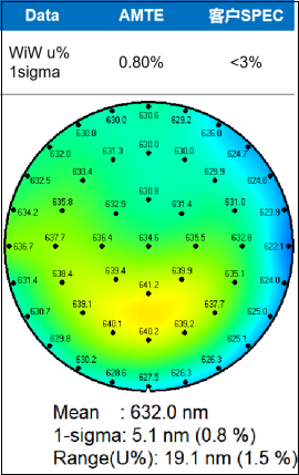
Uniformity analysis
XPS H content analysis

Fourth: Process results and conclusions
The purpose of this process case is to meet the deposition requirements of SiN thin films with high uniformity and low H content. The relevant characterization test results are as follows:
Process effect evaluation
Based on the current set process parameters such as RF power, gas ratio, chamber pressure, and Gap value, the deposited SiN film achieves the expected effect, including:
Homogeneity: The ellipsometer test results show that the uniformity of the prepared SiN film is 0.8%, which meets the customer's technical requirements (<3%).
Film H content: XPS characterization results showed that the Si-H/N-H/Total H content of the prepared SiN film was 2.29%, 11.291%, and 13.582%, respectively, all of which were better than the standard samples provided by the customer with 3.49%, 13.482%, and 16.974%.
Conclusion
The above results indicate that the AMTE SPV 12D 12 inch PECVD equipment exhibits excellent performance in high uniformity and high-quality thin film deposition processes, providing reliable guarantees for the high requirements of device performance consistency and stability in advanced process semiconductor manufacturing.
summary
The SeriC Plasma SPV 12D equipment has met the process requirements on the 12 inch semiconductor manufacturing line. Through technological innovation, market validation, and policy support, we aim to break through key core technologies in semiconductor equipment, promote domestic substitution, gradually narrow the gap with international leading levels, and contribute to the localization of the semiconductor industry. In the future, with the continuous breakthrough of technology and the growth of market demand, AMTE equipment will usher in a broader development space.Editor/Cheng Liting
Comment


 Praise
 Collect
 Comment

 Share
Share


Write something~