 Search


- Total investment of 2.5 billion yuan to build a high-end AI material manufacturing base
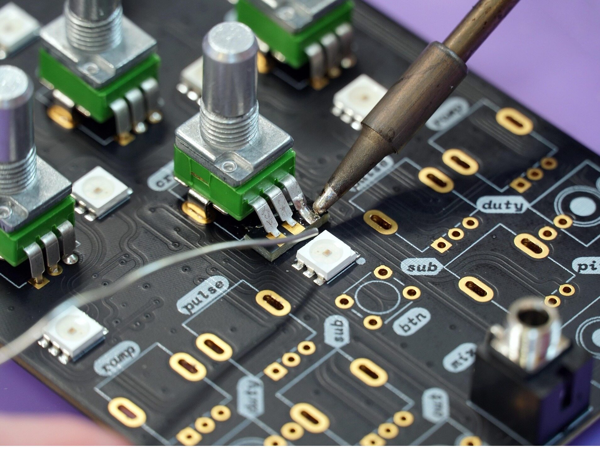
The AI computing power competition has reached a point where the bottleneck is no longer in chip design, but in packaging materials. The global supply of ABF carrier boards is in short supply, and the window for domestic substitution is narrowing. Ipas chose to smash 2.5 billion into Jiangmen Heshan at this node, and the signal is more worthy of attention than the numbers themselves.
Phase II and Phase III linkage targets the urgent need for AI chips
The second phase of construction, with an investment of 1 billion yuan, covers an area of 69 acres and focuses on AI high-speed copper-clad laminates and high-end packaging carrier substrates. It directly connects with four major scenarios: AI chips, data centers, 6G terminals, and satellite link communication, with an annual output value of 1.4 billion yuan after reaching full capacity.
The following three phases of investment amounted to 1.5 billion yuan, covering an area of 78 acres and adding an annual output value of 1.6 billion yuan. The two phases cover a total of 147 acres and 137000 square meters, forming an industrial matrix with the first phase, comprehensively expanding the production capacity of AI high-speed copper-clad laminates and domestic EBF films. EBF film, as a domestic alternative to ABF film, has strategic significance no less than photoresist. Whoever first runs the production capacity will get the ticket to the next round of supply chain.
Rooting in the Bay Area is not a coincidence, it's a calculation
Ipas has been deeply involved in semiconductor packaging materials for eleven years, headquartered in Huangpu, Guangzhou. It is a national high-tech enterprise, a specialized and innovative enterprise in Guangdong Province, and a future unicorn in Guangzhou. It has entered the planning stage for listing. The logic behind choosing Heshan instead of the core area of the Pearl River Delta is clear: Heshan has obvious geographical advantages, mature industrial supporting facilities, efficient business environment, and lower land and labor costs than Guangzhou and Shenzhen, but it has not deviated from the radius of the Bay Area supply chain.
For Jiangmen, Ipas is not just a project, but a key link in extending and supplementing the semiconductor industry chain. Jiangmen has made it clear that it will focus on precise investment promotion for semiconductors, improve park supporting facilities, and build Heshan into a semiconductor material highland in western Guangdong. Keywords: high-tech, AI packaging materials
The domestic substitution of AI packaging materials is not a multiple-choice question, it is a mandatory question. Ipas' 2.5 billion yuan heavy warehouse is essentially gambling on a judgment: in the next three years, the production capacity gap of high-end AI materials will only continue to increase. For Jiangmen, whether it can catch up with this wave of industrial transfer depends on whether the supporting facilities can keep up and whether the policies are implemented effectively. During the window period, there is no waiting for anyone, and those who land first will occupy their positions.Editor/Cheng Liting
Comment

 Praise
 Collect
 Comment

 Share
Share


Write something~