 Search


- Hangzhou Zhongxin Semiconductor breaks through monopoly and successfully delivers to multiple mainstream chip manufacturers
This enterprise, which has been deeply involved in semiconductor silicon wafers since 2002, has completed the transformation from technology introduction to independent innovation in more than 20 years, and its products have entered the global mainstream semiconductor supply chain. On the global semiconductor silicon wafer industry map, the large-size silicon wafer market has long been dominated by Japan's Shin Etsu SUMCO、 Led by international giants such as German Siltronic. For a long time in the past, the dependence of high-end silicon wafers on imports has not fundamentally changed in the Chinese market. According to data, before 2016, the domestication rate of 12 inch silicon wafers was basically 0. In 2024, the domestication rate of 12 inch silicon wafers in China was only about 18% -20%. This supply system dominated by overseas enterprises has led to China's long-term dependence on imported large silicon wafers for key areas such as high-end logic chips and storage chips.
Full size layout breaks foreign monopoly
The technological hard power of Zhongxin Semiconductor is the core support for breaking foreign monopolies. As one of the few domestic enterprises with the ability to supply full-size semiconductor silicon wafers, Zhongxin Wafer has built a complete product matrix covering 4 to 12 inch polished wafers and 8 to 12 inch epitaxial wafers. The dual track layout of polishing and epitaxial wafers has laid a solid foundation for Zhongxin Crystal Circle to achieve large-scale import substitution. In May of this year, the total monthly sales volume of all products of Zhongxin Semiconductor exceeded 1 million pieces, with a compound annual growth rate of 32% in the past five years, reflecting customers' recognition of its products and services.
The independently developed 8-inch gallium nitride epitaxial preparation of heavily doped boron ultra thick polished silicon wafers has achieved significant breakthroughs in the field of high-end substrate materials through multiple core process innovations, successfully breaking the long-term dependence on imports for this type of substrate wafer and filling the relevant technological gap in China. At the 25th China International Industry Expo in 2025, Zhongxin Wafer became the only semiconductor material enterprise that won the CIIF New Material Award, which highly recognized its progressiveness technology.
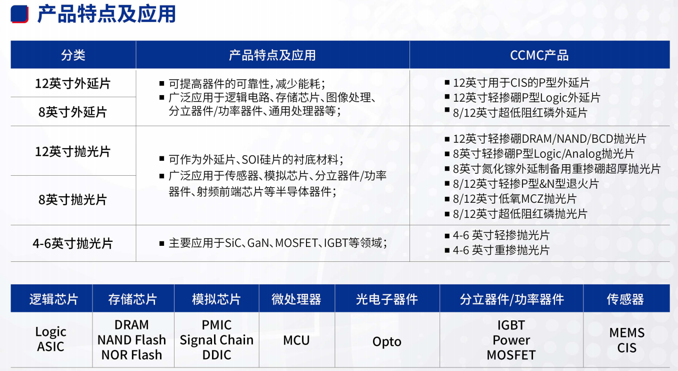
12 inch silicon wafer achieves mass production and delivery
The hardcore of technology ultimately depends on market validation. Zhongxin Wafer has achieved comprehensive breakthroughs in the field of 12 inch silicon wafers, and multiple core products have entered the stage of large-scale production and mass supply. 12 inch lightly doped boron DRAM/NAND polishing wafers have achieved large-scale production and bulk supply in China, and are currently promoting overseas customer sample certification to accelerate integration into the global supply chain system. 12 inch P-type epitaxial wafers, 12 inch N-type heavily doped ultra-low resistance products, and 12 inch lightly doped boron BCD polishing wafers with high technical difficulty for the CIS field have all achieved stable mass production and delivery, meeting the demanding requirements of high-end scenarios such as image sensors and power devices. In the first batch of new material certification in Zhejiang Province in 2025, Zhongxin Wafer's 12 inch silicon single crystal epitaxial wafer was successfully selected, marking that the product has reached the leading level in technology in China and is at the forefront of industrialization and marketization in the industry.

The proportion of R&D investment continues to lead
The growth history of Zhongxin Wafer is a microcosm of the development of China's semiconductor silicon wafer industry. Starting from the introduction of overseas 4-6 inch polishing wafer production lines, and now forming a coordinated development pattern with Hangzhou as the headquarters and six factories in Shanghai, Yinchuan, and Lishui, Zhongxin Wafer has completed a leap from technology introduction to independent innovation. The establishment of the Semiconductor Materials Research Institute in 2021 is a key turning point in Zhongxin's wafer technology roadmap. The research institute is led by top semiconductor materials experts in China, focusing on basic research and industrial applications of 8-12 inch silicon materials.
The R&D expenses of Zhongxin Semiconductor in 2023 and 2024 accounted for 11% and 13% respectively, far higher than the industry average. As of mid-2025, it has obtained nearly 300 authorized patents and is currently applying for nearly 600 invention patents. Zhongxin Semiconductor also actively participates in the formulation of industry standards, contributing to the drafting of 5 national standards and leading or participating in 13 group standards. The national standard for buried silicon epitaxial wafers, which was participated in the compilation, filled the domestic gap and won the first prize of the Technical Standard Excellence Award of the National Semiconductor Equipment and Materials Standardization Technical Committee. Keywords: New Infrastructure News, Semiconductor Latest News

With the listing of the innovation layer on the New Third Board and the launch of guidance from the Beijing Stock Exchange, Zhongxin Semiconductor is ushering in new development opportunities. This Chinese rooted enterprise is fully committed to promoting the goal of full process autonomy, from full-size coverage of large silicon wafers ranging from 4 inches to 12 inches, from single polished wafers to dual wheel drive of polished wafers and epitaxial wafers.
With the continuous explosion of new technologies and market demand such as 5G, artificial intelligence, and the Internet of Things, the cornerstone role of semiconductor silicon wafers will become increasingly prominent. The performance of Zhongxin Semiconductor's monthly sales exceeding one million wafers proves that domestic semiconductor materials are gradually gaining market trust.Editor/Yang Meiling
Comment


 Praise
 Collect
 Comment

 Share
Share


Write something~