 Search


- The fourth phase project of Jinghe Integrated with a total investment of 35.5 billion yuan has officially started in Hefei
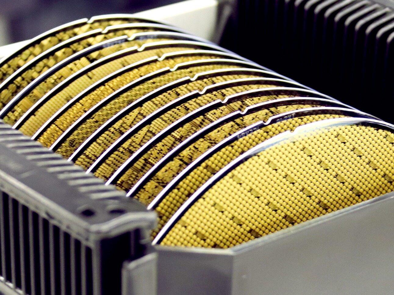
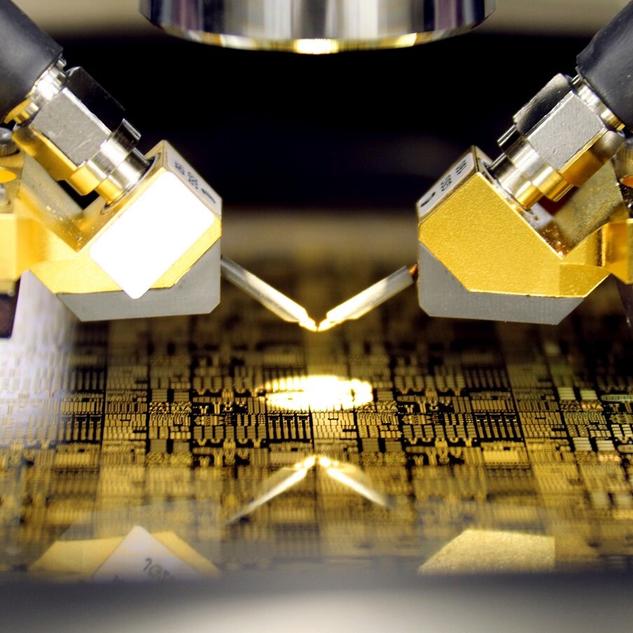
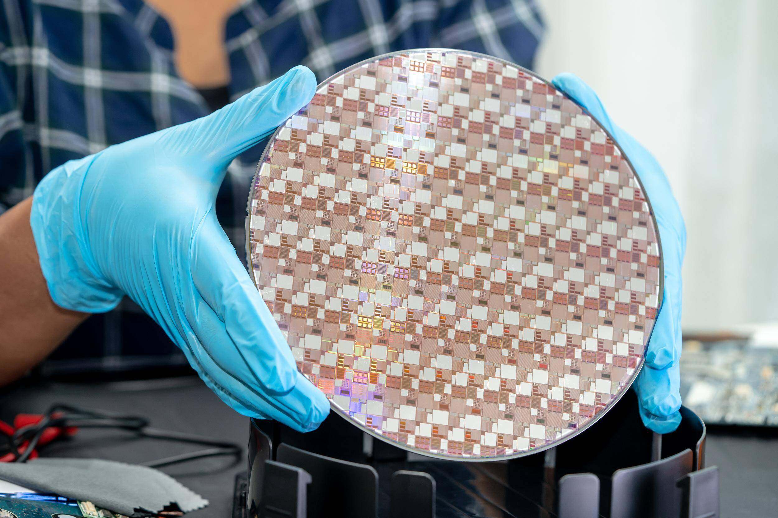
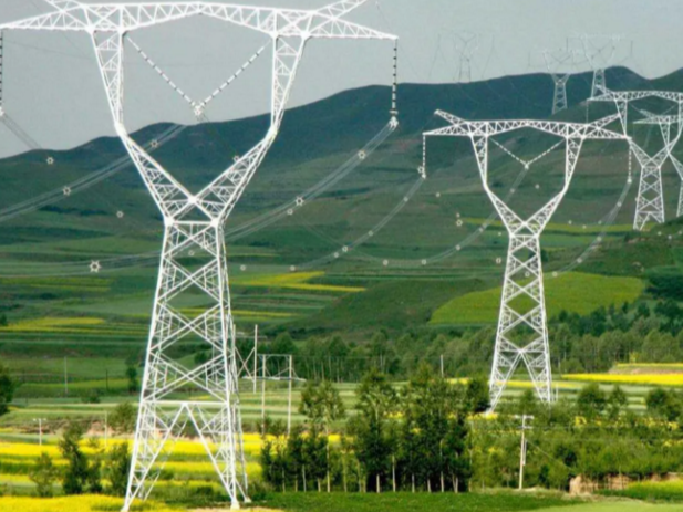
Against the backdrop of increasingly urgent demand for high-performance chips in emerging fields such as artificial intelligence and intelligent vehicles, the core manufacturing process of the domestic semiconductor industry is ushering in a new round of key layout. In January 2026, the Crystal Integration Phase IV project with a total investment of up to 35.5 billion yuan officially started construction in Hefei Xinzhan High tech Zone. The project plans to build a 12 inch wafer foundry production line with a monthly capacity of 55000 pieces, focusing on advanced characteristic processes such as 40nm and 28nm, aiming to provide solid localized manufacturing support for strategic industries such as AI, intelligent automobiles, and high-end displays in China. This investment is not only the largest capacity expansion of JA Solar since its establishment, but also marks the further consolidation and upgrading of Hefei and even Anhui Province's strategic layout in the field of advanced manufacturing of integrated circuits.
Accurately connect with cutting-edge market demands
The core strategic direction of the Crystal Integration Phase IV project is to tackle more competitive characteristic process nodes such as 40nm and 28nm. This project will focus on the layout of CIS image sensors, OLED display drivers, and high-performance logic processes. Its output wafers can be widely used in OLED display panels, AI smartphones and computers, smart cars, and various artificial intelligence terminal devices, accurately matching the current and future market's strong demand for mid to high end chips. Of particular importance is that JA Solar has already completed its technical reserves in the field of logic technology ahead of schedule. Through deep cooperation with customers, multiple 28 nanometer process platforms have been successfully developed, laying a solid foundation for rapid technology introduction and capacity ramp up after the project is put into operation, accelerating the domestic substitution process of related chips.
Steady operation supports strategic expansion
As the third largest wafer foundry in China, JA Solar has achieved a leapfrog growth from catching up to running parallel in just ten years since its establishment in 2015. Starting from a single 150 nanometer process, enterprises gradually tackle more advanced characteristic process nodes such as 55 nanometers, 40 nanometers, and even 28 nanometers; Our business scope has shifted from LCD display driver chip OEM to achieving the top global market share, and then to the top shipment volume of security CIS chips, continuously consolidating our leading advantage in mature and distinctive process areas. The strong performance provides strong support for this large-scale investment: in the first three quarters of 2025, the company achieved a revenue of 8.13 billion yuan, a year-on-year increase of nearly 20%; The net profit attributable to the parent company reached 550 million yuan, with a year-on-year increase of 97.24%. The stable financial performance and clear growth path provide a solid foundation for the high-intensity investment of the fourth phase project. Keywords: New Infrastructure News, New Infrastructure News and Information
Assist in the upgrading of regional cluster energy levels
The selection of the fourth phase project to settle in Hefei Xinzhan High tech Zone will further strengthen the agglomeration effect of the local integrated circuit industry. As an important integrated circuit industry base in China, Hefei has formed a complete industrial chain covering design, manufacturing, packaging and testing. By 2024, the industrial scale will exceed 50 billion yuan and maintain an average annual growth rate of over 20%. As the core carrier area of the industry, Xinzhan High tech Zone provides guarantees for the landing of major projects through preferential policies such as land and supporting facilities. Jinghe Integration's increased investment this time will generate stronger synergies with upstream and downstream enterprises in the region, helping Hefei build a more complete and robust "design manufacturing packaging" industry loop, enhancing the overall competitiveness and risk resistance of the industry chain. The project is expected to achieve equipment relocation and production in the fourth quarter of 2026, and reach full production in the second quarter of 2028. At that time, it will significantly enhance China's independent and controllable production capacity in the field of advanced characteristic processes, and contribute key forces to ensuring the security and stability of the national integrated circuit industry supply chain. (This article is from the official website of Jian Dao www.seetao.com. Reproduction without permission is prohibited, otherwise it will be prosecuted. Please indicate Jian Dao website+original link when reprinting.) Jian Dao website New Infrastructure column editor/Gao Xue
Comment


 Praise
 Collect
 Comment

 Share
Share


Write something~