 Search


- New chip technology landing, breaking the physical limitations of traditional Moore's Law
- The formation of a new semiconductor track helps domestic industries achieve lane changing overtaking
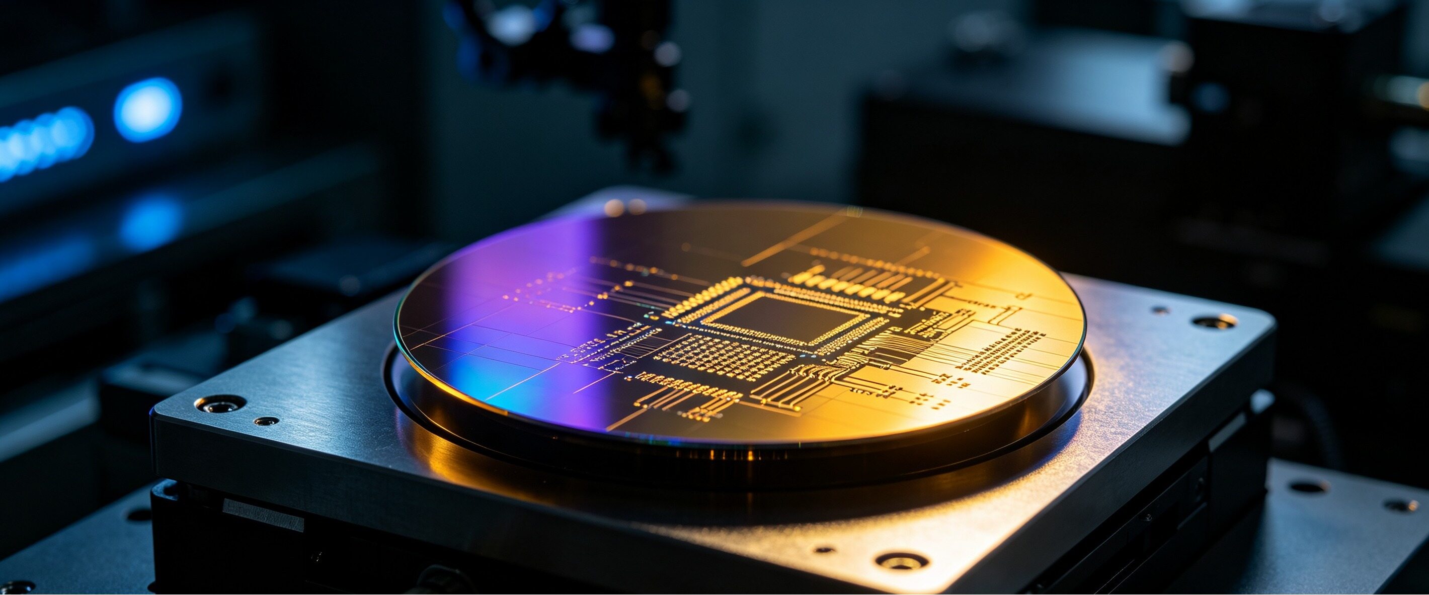
The wafer under the microscope slowly flows, as if weaving the future at the atomic scale. As traditional silicon-based chips approach their physical limits, an 8-inch production line in Shanghai quietly connects, pushing the thin two-dimensional materials in the laboratory towards industrialization for the first time.
Breaking through laboratory barriers
On July 9, 2026, Yuanjiwei Technology's 8-inch 2D semiconductor process line in Shanghai was fully connected, becoming the first 2D semiconductor engineering demonstration production line in China. This marks the formal industrialization of the two-dimensional semiconductor research achievements in China over the past decade. In the past few decades, the improvement of chip performance has relied on reducing transistor size and iterating according to Moore's Law. But as the process approaches the physical limit, the leakage problem intensifies, the difficulty and cost of the process increase significantly, and the development of traditional silicon-based chips encounters bottlenecks. Two dimensional semiconductors have atomic level ultra-thin structures that can effectively suppress leakage and reduce process difficulty, making them a recognized new technology route for advanced processes below 1 nanometer in the industry.
Previously, the domestic two-dimensional semiconductor achievements in China mostly remained at the stage of university laboratories, with high sample accuracy but unable to be mass-produced, resulting in significant engineering gaps. The original Jiwei team has gone through ten years of research and development to integrate the entire chain technology, but has long lacked industrial production lines that can be mass-produced to undertake the transformation of achievements. The 8-inch production line connection this time has bridged the gap between scientific research and mass production, forming a complete engineering system from materials, design to wafer production, which can directly undertake scientific research project wafer trial production.
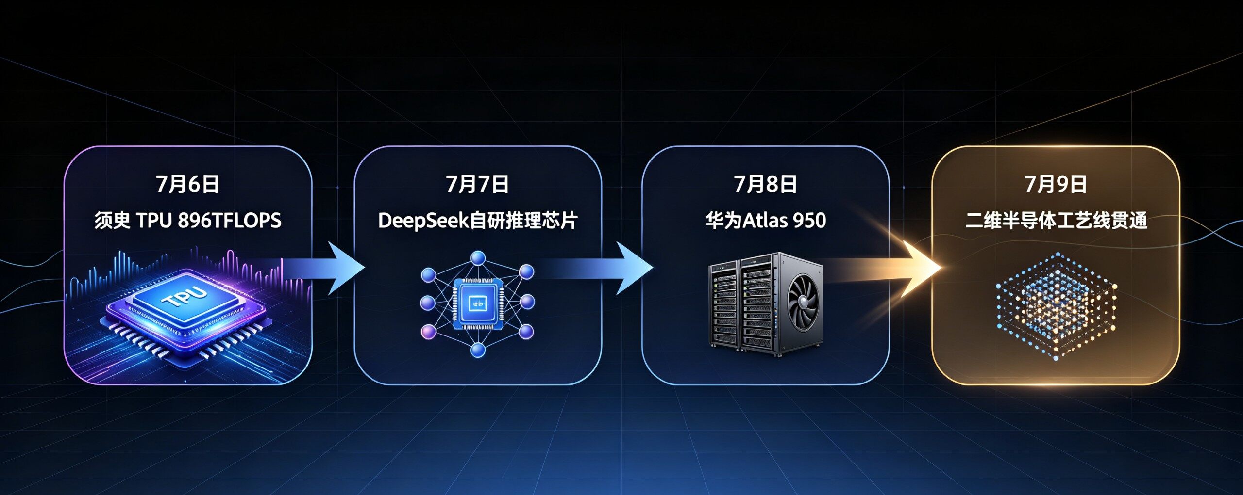
Shanghai has already taken the lead in this field. In 2025, the world's first two-dimensional semiconductor architecture processor will be released, and ultra-low leakage transistors and new storage chips will be introduced one after another. In January 2026, the two-dimensional semiconductor communication system successfully completed space in orbit verification, and its technological maturity continues to improve. The international competition for two-dimensional semiconductors is becoming increasingly fierce, and Shanghai has listed it as a key industry for the future, building a closed-loop ecosystem of research and development, pilot testing, and mass production, and continuously promoting the implementation of technology.
Leading the world in terms of craftsmanship level
At the opening ceremony, Yuanjiwei released a 500 nanometer process design toolkit that is compatible with 8-inch production lines, and fully opened up OEM wafer services. The process design toolkit is the core bridge between chip design and manufacturing, supporting mainstream design tools and ensuring efficient implementation and production of R&D solutions. This process is the first two-dimensional semiconductor full process intellectual property solution in China, with an overall yield rate of over 99.99% and multiple indicators breaking international records. Its performance is close to that of silicon-based processes of the same level, and it can support large-scale circuit design and wafer manufacturing.

After the opening of the production line, universities such as Tsinghua University, Peking University, and Shanghai Jiao Tong University have successively carried out school enterprise cooperation, and scientific research achievements have been quickly implemented and recorded, completely changing the previous situation of only laboratory research. Two dimensional semiconductors have unique advantages such as radiation resistance, high sensitivity, and flexible transparency, and can be widely used in cutting-edge fields such as radio frequency communication, brain computer interfaces, optoelectronic sensing, and quantum computing. It is expected that the global market size will reach 30 billion to 50 billion US dollars by 2035, with enormous industrial potential.
Anchor high-end process advancement
According to the plan, in the second half of 2026, the project will rely on an 8-inch production line to connect equivalent 90 nanometer processes, complete reliability verification, and promote technological industrialization upgrading. Standardized foundry services for silicon-based processes will be launched in 2027. The company expects to achieve a key breakthrough by 2029, relying on domestically produced lithography machines in China to create a nationwide two-dimensional semiconductor manufacturing solution that does not require EUV equipment and is equivalent to 5 nanometers. At the same time, through material stacking and new power supply technologies, the integration and performance of chips are continuously improved. Keywords: 2D semiconductor, 8-inch process line, chip industrialization
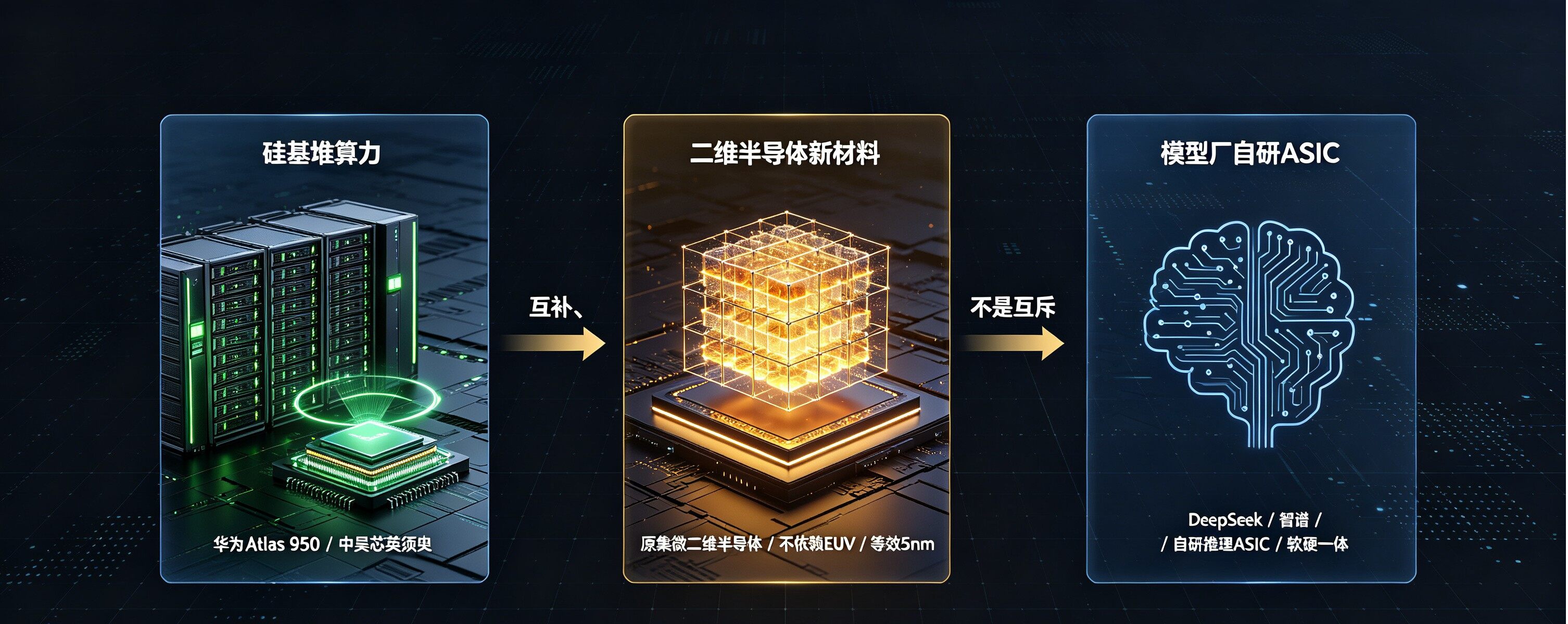
With the support of policies, industries, and capital from multiple sources, China's domestic two-dimensional semiconductors have moved beyond the laboratory and entered a critical period of industrialization. With independent and controllable technology, unrestricted equipment, and continuously improving ecology, China has the advantage of changing lanes and overtaking in the new semiconductor track, which is expected to break the monopoly of overseas high-end chip technology.Editor/Gong Ziwei
Comment



 Praise
 Collect
 Comment

 Share
Share


Write something~