 Search


- Chip competition shifts to system game, continuing the development space of Moore's Law
- AI Reshaps Semiconductor Evaluation System, Mask Ratio Becomes an Important Measurement Indicator
For over 60 years, nanotechnology has been the core measurement standard for semiconductors, and the reduction in transistor size determines chip performance. In the era of AI, mask multiplier has become the second key benchmark for the industry. At the OCP Asia Pacific Summit on August 11th, TSMC revealed that the 5.5x mask CoWoS has been mass-produced with a yield rate of over 98%, and will strive to meet the 14x mask specification in the future.
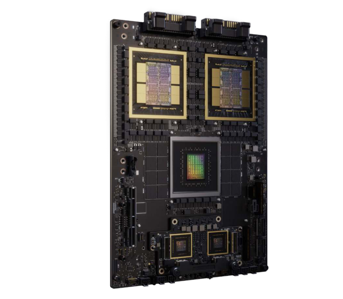
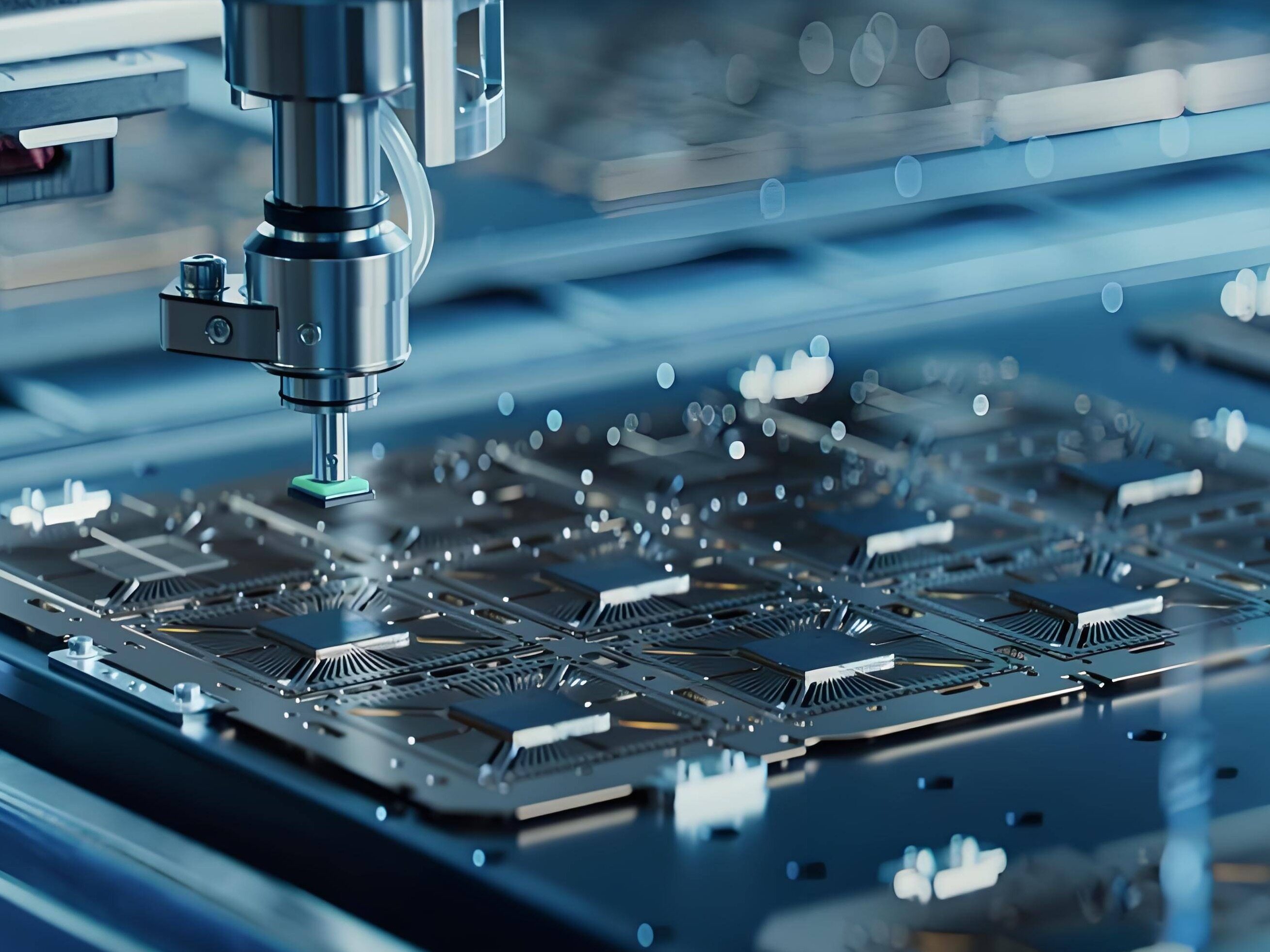
According to the technical roadmap, the 14 fold mask CoWoS is planned to be mass-produced in 2028, which can integrate 10 computing chips and 20 HBMs, and will continue to break through the size limit in 2029. The 14 fold photomask is not a single photomask that magnifies by 14 times, but rather covers more than ten photolithography areas through packaging intermediate layers, rewiring, and chip integration. The overall trend of advanced packaging is showing a continuous amplification.
The logic behind the oversized packaging
Relying on process compression to fit more transistors into a single chip has a physical ceiling and will encounter the mask limit brought by lithography machines. Nvidia Blackwell adopts a dual core grain architecture, which is limited by this physical boundary. Chiplet chip splitting solves the size constraint of a single chip, but also brings the challenge of bandwidth interconnection among multiple chips. The AI big model drives the synchronous increase in the number of computing chips and HBMs, requiring low latency and high bandwidth to achieve a large number of chip interconnections. Thus, a contradictory phenomenon emerged: a single chip was dismantled and reduced in size, while the entire computing power system grew larger and larger. The 14 times mask CoWoS aims to restructure dozens of different functional chips into a set of super AI chips.
Giant innovates packaging architecture
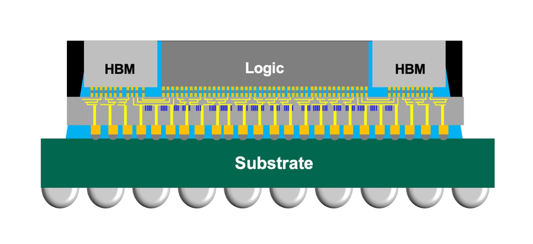
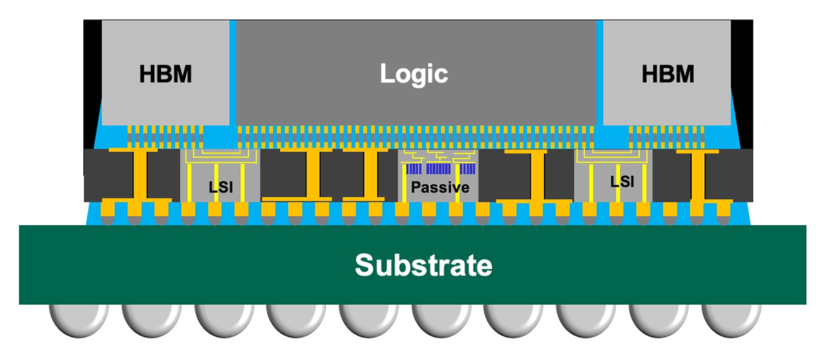
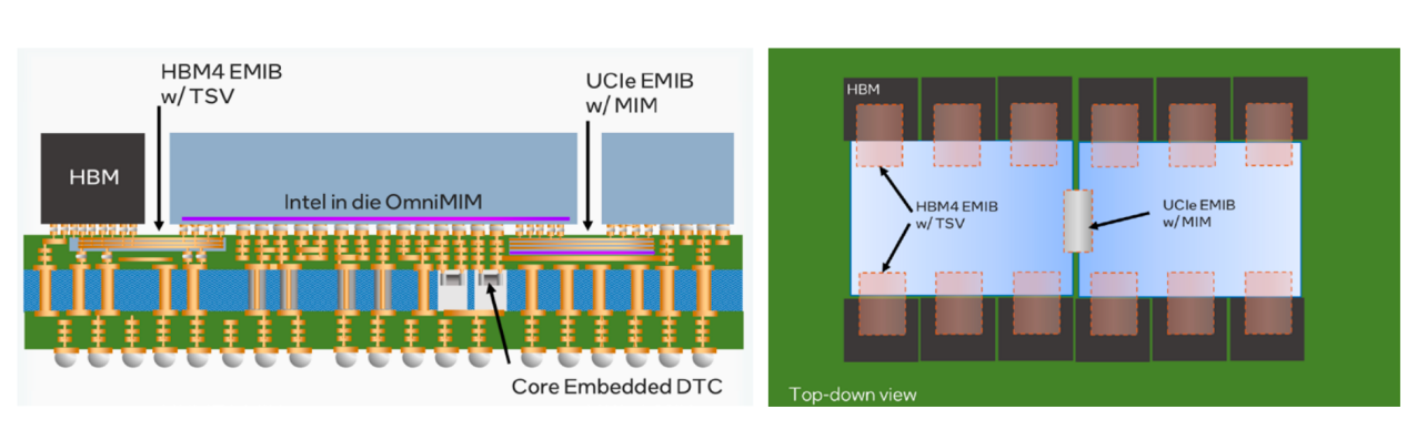
The packaging has moved from several times to 14 times the size of the photomask, not simply by enlarging the area, but by restructuring the underlying architecture. TSMC's traditional CoWoS-S relies on a single silicon intermediate layer, and as the size increases, the cost and yield pressure suddenly increase. CoWoS-L will be locally embedded with silicon interconnect units, while the rest will use low-cost expandable plastic packaging and rewiring to balance performance and yield. Intel EMIB and Samsung I-CubeE have similar ideas, abandoning the entire large silicon intermediate layer and only retaining the silicon structure at high-speed interconnect positions to break through size limitations and control costs. Although the three major manufacturers have different technical solutions, their core ideas are highly similar.
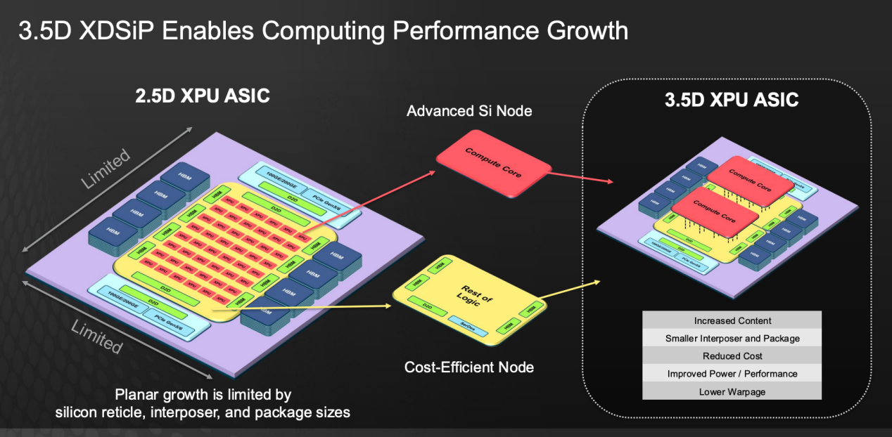
The expansion of planar packaging will encounter bottlenecks in size, heat dissipation, and signal delay, and the industry has opened up a 3D vertical stacking route. 2.5D is responsible for horizontally arranging chips, while 3D ICs are vertically stacked to enhance computing power per unit area. Broadcom XDSiP integrates 2.5D and 3D stacking, mixing different processes to reduce costs and alleviate chip warping. TSMC SoIC hybrid bonding significantly improves interconnect density and energy efficiency. In the future, AI chips will be horizontally extended in two dimensions and vertically stacked in three dimensions, and will be integrated into the entire 3D Fabric system.
14 times mask packaging faces multiple challenges including yield, warpage stress, heat dissipation, and supply chain. Multiple chips are integrated, and the failure of a single chip will result in overall scrap. Different chips also have performance differences, requiring Die Matching die matching to screen and adapt chips. The thermal expansion and contraction of various materials cause warping stress, requiring the participation of cover plates and thermal interface materials in structural design, and promoting collaborative optimization of system technology. High density integration brings about power consumption and hotspot issues, and the coupling of heat, force, and electricity must be verified in conjunction with the entire system. At the same time, ABF carrier board HBM、 Special materials and equipment will become new bottlenecks in the supply chain, requiring synchronous upgrading of the entire industry chain. Keywords: chip, semiconductor, system integration
The industry is undergoing a new transformation
The semiconductor industry is shifting from transistor miniaturization to system integration. Advanced processes are no longer the only source of computing power, relying on processes Chiplet、HBM、 Advanced packaging and 3D stacking jointly continue Moore's Law. The competition for chips has shifted from competing for single chip capabilities to developing comprehensive system integration capabilities. In the first half of the industry, we focus on single large chips, while in the second half, we focus on multi chip large systems.Editor/Gong Ziwei
Comment


 Praise
 Collect
 Comment

 Share
Share


Write something~