 Search


- Project focuses on filling the gaps in mass production of compound semiconductors

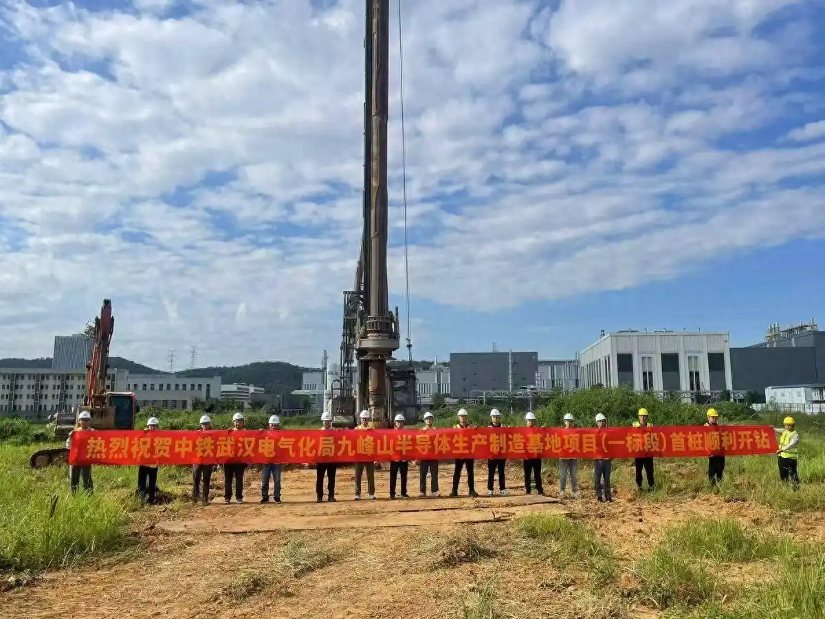
On July 20, 2026, in Donghu High tech Zone, Wuhan, the rotary drilling rig started smoothly, and the first pile of Jiufengshan Semiconductor Manufacturing Base was successfully drilled. This marks the key puzzle of the Optics Valley compound semiconductor industry from research and development to mass production, officially entering the substantive construction stage.
Starting from 120000 square meters
The project is located in the core science and technology innovation area of Optics Valley. The first section of the implementation includes two research and development office buildings and a 15 story shift dormitory building, with a total construction area of approximately 120000 square meters. The total investment of the project is about 5.2 billion yuan, with a planned construction period of 730 days. The long-term total construction area will reach 353000 square meters, which can support the landing of advanced production lines such as 8-inch MEMS and 12 inch silicon-based gallium nitride.
Optics Valley started from the optoelectronics industry and built the world's largest and most advanced compound semiconductor pilot platform based on the Jiufengshan Laboratory. It has deeply collaborated with nearly 600 industry chain partners worldwide, driving more than 70 landing enterprises, and the scale of the city's compound semiconductor industry has exceeded 40 billion yuan. But the shortcomings of mass production carriers have always existed. The mission of Jiufengshan Manufacturing Base is to make up for this link - to enable chip research and development results to directly enter the mass production line from the laboratory, and completely connect the entire chain.
The core puzzle of the billion dollar industrial block
The Jiufengshan Science and Technology Park, where the project is located, is a core component of the 14 square kilometer compound semiconductor industry innovation block in Optics Valley. The park has planned 168000 square meters of incubation acceleration and manufacturing base, striving to introduce and cultivate 100 upstream and downstream enterprises within 3 years. Keywords: semiconductor, high-tech

Since 2026, Optics Valley has established a government investment fund group worth 89 billion yuan, and 24 compound semiconductor projects have signed contracts and settled down. With the full construction of Jiufengshan Manufacturing Base, the goal of Optics Valley's billion yuan compound semiconductor industry is moving from planning drawings to construction sites.Editor/Cheng Liting
Comment





 Praise
 Collect
 Comment

 Share
Share


Write something~