 Search


- Chips that balance low cost and low power consumption, suitable for various industrial and intelligent terminal scenarios
- Innovative chip architecture eliminates data transmission losses and achieves a leapfrog improvement in computing speed
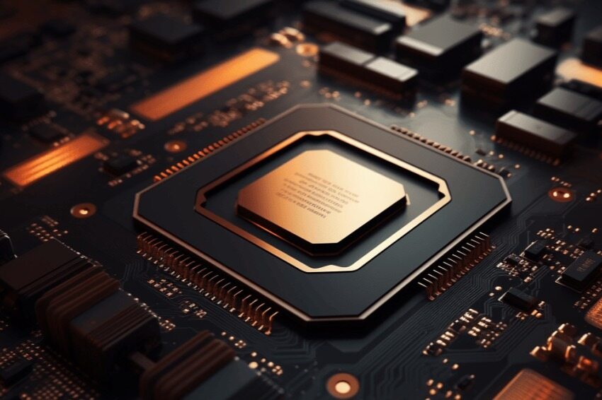
When the torrent of data is running between the two poles of storage and computing, the power consumption wall of chips has quietly approached its limit. This blow severed decades long architectural ties and allowed computing to return to storage itself. In the nanoscale battlefield, a silent revolution about computing power efficiency is reshaping the future of intelligence from the underlying logic.
New chip officially released to the public
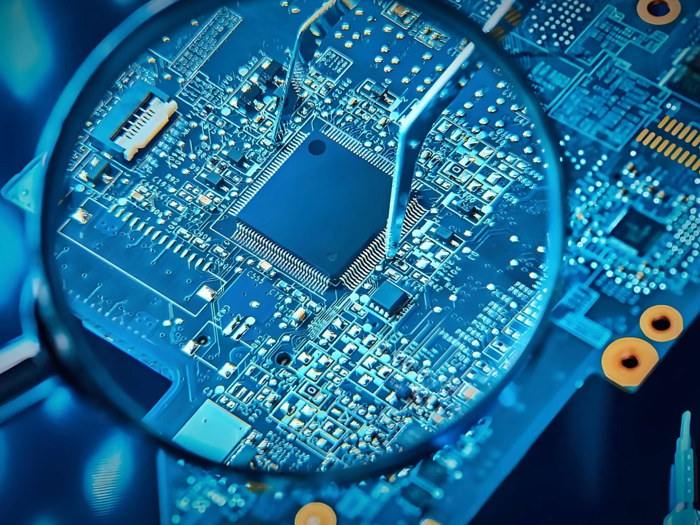
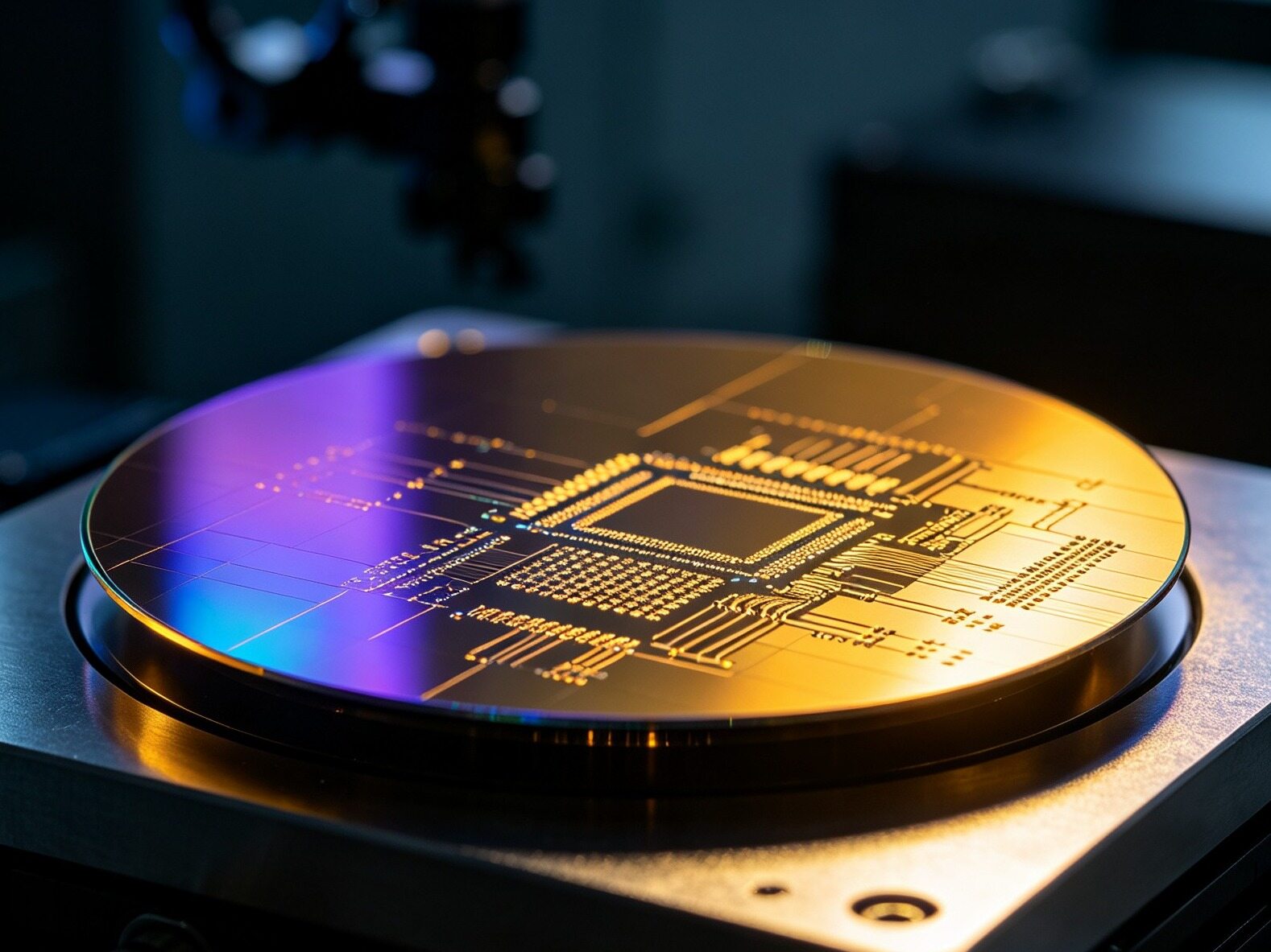
In early July 2026, Peking University partnered with the Shanghai Institute of Microsystems, Chinese Academy of Sciences to launch a 40 nanometer phase change storage and computing integrated chip. This product abandons the traditional storage and computing separation architecture, completely solving the high power consumption and high latency problems caused by data transmission. The chip only takes 2.12 milliseconds to complete a single matrix multiplication operation, which is nearly 50 times faster than mainstream mid-range GPUs in processing the same task.
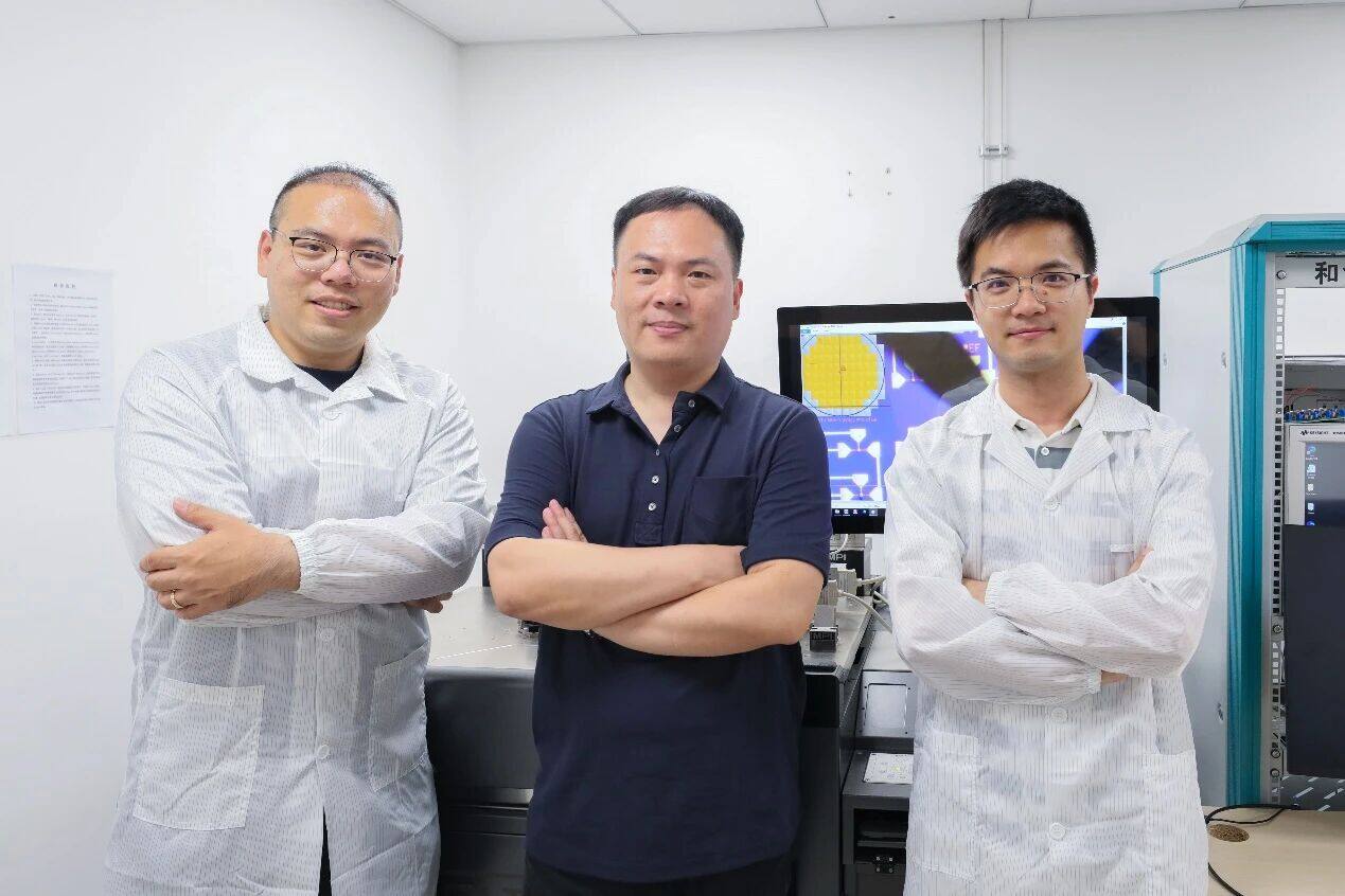
Architectural innovation reduces usage costs
The computing and storage hardware of traditional computing chips are independent of each other. When conducting large-scale model inference, 3D reconstruction, and industrial simulation work, the data transmission link consumes a large amount of power and computing resources. This memory computing integrated chip can directly complete multiplication and addition operations inside the storage array, effectively reduce bandwidth occupation and energy consumption, and adapt to a variety of application scenarios such as low-power edge computing, local industrial intelligent reasoning, and on-board intelligent AI.
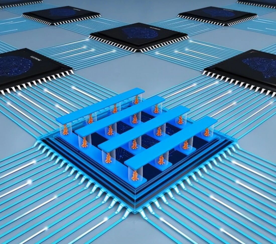
This chip does not require large capacity high-speed storage accessories, and the entire hardware procurement cost can be reduced by more than 40%. Pilot work has been carried out in two major scenarios: industrial quality inspection and digital twin. The R&D team has simultaneously launched an operator library adapted to China's self-developed large models, reducing the adaptation investment for enterprise landing applications. Keywords: integrated storage and computing chip GPU、 Domestic large model
Industry welcomes opportunities for technological change
In the long run, the integrated storage and computing technology will change the original competitive landscape of the edge computing market, and the lightweight local computing and industrial intelligent computing tracks will usher in technological upgrading dividends. China's self-developed storage and computing integrated chip has achieved a key performance breakthrough, opening up a new technological development path for the low-power edge computing industry.Editor/Gong Ziwei
Comment



 Praise
 Collect
 Comment

 Share
Share


Write something~